
SCIENTIFIC RESEARCH
Nano Research Center
Team Introduction
Micro and nano optics team is committed to micro and nano optical process research and development, optical device development, with micro and nano optical process and optical device simulation design, processing, testing and packaging capabilities. The team has undertaken key national key projects such as the National Key research and Development Plan, the National Natural Science Foundation Regional Innovation and Development Joint Fund, etc. Micro-nano optical devices such as on-chip optical phased array, polarization switchable directional coupler, subwavelength periodic waveguide array, multifunctional photonic integrated chip, ultra-low power optical communication chip, wavelength multiplexing chip, and many thin film lithium niobate optical waveguide devices have been successfully developed. He has published many papers in domestic and foreign journals such as "Nat.Commun." "Phys. Rev. Lett." "Adv. Mater." "Light Sci.Appl." and obtained a number of authorized invention patents.

Micro Nano Process Development
-
Process research and development
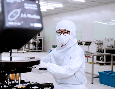
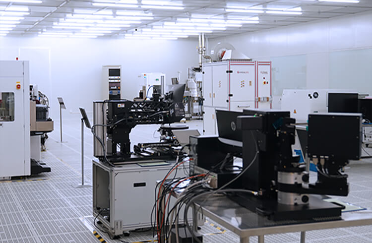
The center can provide process research and develop- ment services and various process testing services related to wafer manufacturing, such as lithography, coating development, injection, oxidation diffusion, epitaxial growth, cleaning, film deposition, etching, chemical mechanical grinding, etc.
-

Process Design Kit (PDK)
The center has developed a series of silicon optical passive devices, such as waveguides with different etching depths, fiber couplers, shard/couplers, multi-channel multiplexers, thermal phase shifters, etc., and has also developed a series of high-speed active devices, such as phase modulators of carrier dissipation
-
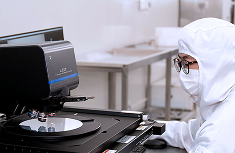
Test package
The center can provide optoelectronic chip testing and packaging, including electrical packaging, optical packaging, and optical performance testing of optoelectronic devices and links on chips and wafers.
Optoelectronic Device Development
-

Development of silicon based optical devices
-
Silicon based device design
The center has professionals engaged in the design of silicon-based optical waveguides and devices, and can provide simulation and optimization design services for various silicon-based optical devices.
-
Silicon based optoelectronic device processing
The center has a team of process engineers and the process and testing equipment required for the processing of silicon-based optical devices, and has the professional processing capability of silicon-based optoelectronic devices.
-
-
Technology of lithium niobate thin film photoelectric device
-
Device design
The center has professionals engaged in thin film lithium niobate optical waveguide and device design, and can provide simulation and optimization design services for various thin film lithium niobate optical devices.
-
Technology of thin film lithium niobate optical device
The center has a team of process engineers and the process and testing equipment required for the processing of thin film lithium niobate optical devices, and has professional processing capabilities for thin film lithium niobate optical waveguides and optoelectronic devices.
-